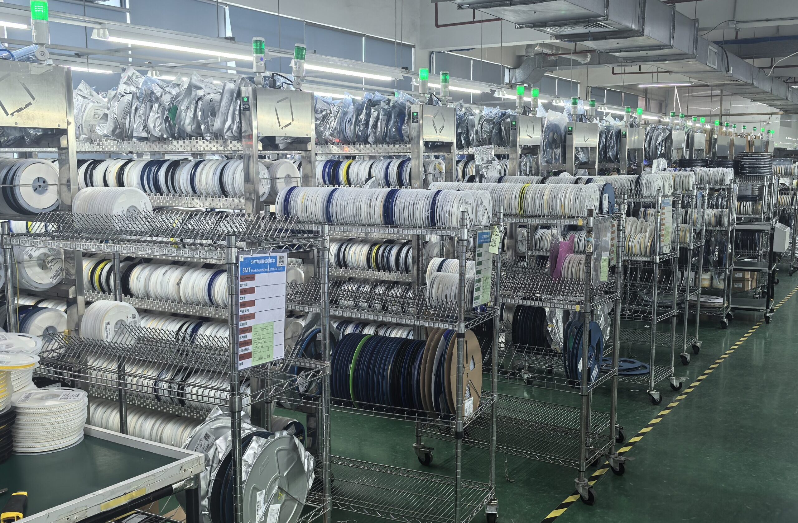
What is SMT chip processing?
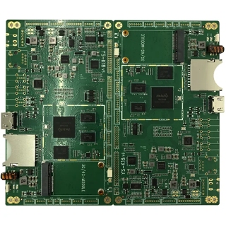
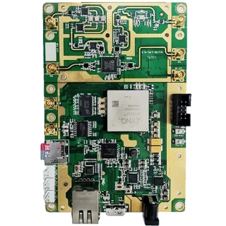
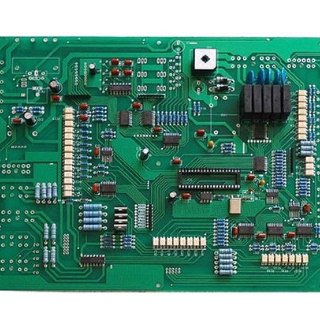
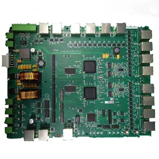
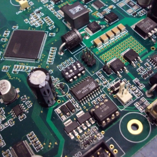
SMT chip processing is a method of assembling electronic circuits that involves soldering surface mount components (e.g., chips, resistors, capacitors, etc.) to the surface of a printed circuit board (PCB). The components are typically small, and the soldering process is carried out with the help of a specialized machine known as a pick and place machine, which precisely places the components onto the PCB.
How is SMT chip processing different from through-hole technology?
Through-hole technology, which involves inserting components into holes on a PCB and soldering them in place, is another method of assembling electronic circuits. In contrast, SMT chip processing involves placing components on the surface of the PCB rather than inserting them into holes. SMT components are better suited for use in smaller, more compact electronic devices because they are smaller and more densely packed than through-hole components.
What are the advantages of SMT chip processing?
Here are some of the benefits of using SMT chip processing:
Because SMT components are smaller and more densely packed than through-hole components, they can be used to make smaller and more compact electronic devices.
Because the pick and place machine can place multiple components at once with high precision, SMT chip processing is faster and more efficient than through-hole technology.
SMT components are more vibration and shock resistant than through-hole components, making them more suitable for use in rugged or mobile applications.
What are the challenges of SMT chip processing?
There are several difficulties with SMT chip processing:
Because SMT components are much smaller than through-hole components, they are more difficult to handle and install on the PCB.
Soldering SMT components necessitates the use of specialized equipment and techniques that can be difficult to master.
Because even small amounts of dust or other contaminants can affect the quality of the soldering process, SMT chip processing is more sensitive to contaminants and defects.
What equipment is used in SMT chip processing?
Several pieces of equipment are frequently used in SMT chip processing:
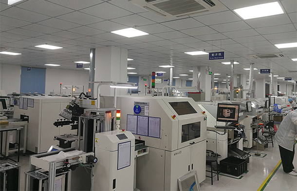
Machine for picking and placing: A machine that precisely places components on the PCB.
Oven for reflow: A machine that rapidly heats the PCB and components, melting the solder and causing it to flow around the components, forming a strong connection.
Solder paste stencil: A thin sheet of metal with holes in it used to apply a precise amount of solder paste to the PCB.
Solder paste is a thick, pasty mixture of solder and flux used to hold components in place and speed up the soldering process.
What is the process of SMT chip processing?
The SMT chip processing process typically includes the following steps:
Preparation: The PCB is cleaned and prepared before beginning the soldering process to ensure that it is ready for component placement and the soldering process. Cleaning the PCB with a solvent or specialized cleaning solution to remove any dirt, dust, or contaminants on its surface is typical, followed by treating the PCB with a flux to facilitate the soldering process.
Printing: During the printing process, a thin sheet of metal called a solder paste stencil is used to apply a precise amount of solder paste to the PCB. The stencil is cut with a pattern of holes that corresponds to the placement of the components on the PCB. Using a squeegee or other similar tool, a thin layer of solder paste is applied to the stencil after it has been placed over the PCB. The solder paste flows through the stencil holes and onto the PCB, forming a pattern that corresponds to the component placement.
Placement: Pick and place machines are used to precisely place components on the PCB in the correct positions. The machine picks up and places the components on the PCB with high precision using a series of robotic arms and vision systems. The machine is programmed with the correct component placement coordinates and uses its vision systems to locate the correct positions on the PCB.
Reflow: The PCB and components are placed in a specialized oven known as a reflow oven during the reflow process. The oven raises the temperature of the PCB and components to a high level, typically between 180 and 260 degrees Celsius, depending on the type of solder used. The solder paste on the PCB begins to melt and flow around the components as the temperature rises, forming a strong connection between the components and the PCB. During the reflow process, the temperature is carefully controlled to ensure that the solder flows properly and forms a reliable connection without damaging the components or the PCB.
After the reflow process is finished, the PCB is cooled and removed from the oven. After that, the soldered joints are inspected to ensure that they are properly formed and that all components are properly placed and soldered. This is usually accomplished through the use of a combination of automated and manual inspection methods, such as visual inspection, x-ray inspection, and automated optical inspection (AOI). Any defects discovered during the inspection process can be corrected by reworking the PCB, which entails removing and resoldering the faulty components.
Preparation: The PCB is cleaned and prepared for the soldering process.
Yes, preparation is a critical step in the SMT chip manufacturing process. Before beginning the soldering process, the PCB must be cleaned and prepared to ensure that it is ready for component placement and the soldering process.
To remove any dirt, dust, or contaminants that may be present on the PCB's surface, it is typically cleaned with a solvent or a specialized cleaning solution. This is significant because even trace amounts of contaminants can degrade the soldering process and result in defects in the finished product.
A flux, a chemical agent that aids in the removal of oxides and other contaminants from the surface of the PCB and its components, may also be applied to the PCB. Flux also aids in the soldering process by lowering the surface tension of the molten solder and allowing it to flow more freely.
After the PCB has been cleaned and prepared, it is ready for printing, component placement, and the reflow process. Any defects or contaminants found on the PCB during the inspection process can be detected and corrected by reworking the PCB, which involves removing and resoldering the faulty components.
Printing: Solder paste is applied to the PCB using a solder paste stencil.
Yes, printing is an important step in the SMT chip processing process. A thin sheet of metal called a solder paste stencil is used during the printing process to apply a precise amount of solder paste to the PCB.
The solder paste stencil is cut with a pattern of holes that corresponds to the location of the components on the PCB. A thin layer of solder paste is applied to the stencil with a squeegee or similar tool after it has been placed over the PCB. The solder paste flows through the stencil holes and onto the PCB, forming a pattern that corresponds to the component placement.
The printing process is critical for ensuring that the proper amount of solder paste is applied to the PCB and in the correct locations. During the inspection process, any defects in the solder paste application, such as excess or insufficient solder, can be detected and corrected by reworking the PCB, which involves removing and resoldering the faulty components.
Placement: The pick and place machine places the components onto the PCB in the correct positions.
Yes, the placement process is critical in SMT chip processing. A pick-and-place machine is used during the placement process to accurately place the components onto the PCB in the correct positions.
The pick and place machine uses a series of robotic arms and vision systems to pick up and place the components onto the PCB with high precision. The machine is programmed with the correct placement coordinates for each component, and it uses its vision systems to locate the correct positions on the PCB.
The pick and place machine is a key piece of equipment in the SMT chip processing process, as it allows for high-precision placement of the components onto the PCB. This is critical for ensuring that the finished product is of high quality and reliability. Any defects in component placement can be detected during the inspection process and corrected by reworking the PCB, which involves removing and resoldering the faulty components.
Reflow: The PCB and components are placed in a reflow oven, where they are heated to a high temperature, melting the solder and causing it to flow around the components.
Yes, the reflow process is an important step in the fabrication of SMT chips. The PCB and components are placed in a specialized oven called a reflow oven during the reflow process. The oven raises the temperature of the PCB and components to a high level, typically between 180 and 260 degrees Celsius, depending on the type of solder used.
The solder paste on the PCB begins to melt and flow around the components as the temperature rises, forming a strong connection between the components and the PCB. During the reflow process, the temperature is carefully controlled to ensure that the solder flows properly and forms a reliable connection without damaging the components or the PCB.
Inspection: The completed PCB is inspected to ensure that all components are correctly placed and soldered.
Yes, inspection is a critical step in the SMT chip manufacturing process. The completed PCB is inspected after the reflow process to ensure that all components are correctly placed and soldered. This is usually accomplished through the use of a combination of automated and manual inspection methods, such as visual inspection, x-ray inspection, and automated optical inspection (AOI).
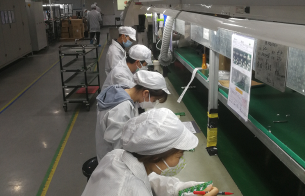
During visual inspection, a technician examines the PCB with a magnifying glass or microscope for defects such as misalignment, solder balls, and excess or insufficient solder. X-ray inspection involves inspecting the PCB with a specialized x-ray machine for defects that are not visible to the naked eye, such as solder voids and misaligned components. Cameras and computer software are used to automatically scan the PCB for defects, allowing for faster and more accurate inspection than manual methods.
What are some common defects in SMT chip processing
Solder bridges occur when a blob of excess solder connects two adjacent pads or components.
Solder balls are small balls of excess solder that form on the PCB's surface.
Open circuits: An open circuit occurs when a component is not properly soldered to the PCB.
Shorts happen when two components or pads are soldered together by mistake, resulting in a short circuit.
Misalignment occurs when a component is not correctly placed on the PCB, resulting in an incorrect or faulty connection.
Shorts happen when two components or pads are soldered together by mistake, resulting in a short circuit.
Misalignment occurs when a component is not correctly placed on the PCB, resulting in an incorrect or faulty connection.
Solder voids are small areas within a soldered joint that are not filled with solder, resulting in a weak connection.
Insufficient solder: When there is insufficient solder on the PCB, it results in a weak or unreliable connection.
Excess solder: When there is too much solder on the PCB, it causes a sloppy or unreliable connection.
These flaws can be caused by several factors, such as faulty equipment, improper solder paste application, or operator error. They can be detected and corrected during the inspection process, or they can be avoided entirely by adhering to proper procedures and employing high-quality materials and equipment.