

What is a PCB Assembler?
Printed Circuit Board (PCB) assembly is a critical process in the manufacturing of electronic devices. It involves attaching electronic components to the PCB, which serves as the backbone of electronic circuits. This blog will explore the intricacies of PCB assembly, covering everything from the basics to advanced techniques, and providing valuable insights for professionals and hobbyists alike.
Understanding PCB Assembly
PCB assembly, often abbreviated as PCBA, is the process of soldering or mounting electronic components onto a PCB. This process transforms a bare board into a functional piece of electronic equipment. The primary methods of PCB assembly include Surface Mount Technology (SMT) and Through-Hole Technology (THT).
- Surface Mount Technology (SMT): SMT involves placing components directly onto the surface of the PCB. This method is highly efficient and allows for the placement of small and lightweight components. SMT is favored in modern electronics due to its ability to accommodate high-density component placement.
- Through-Hole Technology (THT): THT involves inserting component leads through holes in the PCB and soldering them in place. This method is more robust and is often used for components that require mechanical stability, such as connectors and large capacitors.
Key Steps in PCB Assembly
- Solder Paste Application: The first step in SMT assembly is applying solder paste to the PCB. This is typically done using a stencil that matches the PCB layout. The paste, a mixture of tiny solder balls and flux, is applied to the areas where components will be mounted.
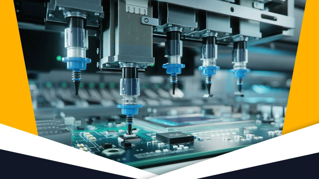
- Pick and Place: In this step, automated machines place electronic components onto the solder paste-covered PCB. These machines are highly precise and can place thousands of components per hour.
- Reflow Soldering: After the components are placed, the PCB is passed through a reflow oven. The heat melts the solder paste, creating solid solder joints that connect the components to the PCB.
- Inspection and Quality Control: Post-reflow, the assembled PCB undergoes various inspections to ensure all components are correctly placed and soldered. Automated Optical Inspection (AOI) and X-ray inspection are commonly used techniques.
- Through-Hole Component Insertion (if applicable): For THT, components are manually or automatically inserted into the PCB holes. The leads are then soldered to secure the components.
- Final Testing: The assembled PCB is tested to ensure it functions as intended. Functional testing and in-circuit testing are standard procedures to verify the performance and reliability of the PCB.
Challenges in PCB Assembly
PCB assembly is a complex process with several challenges:
- Miniaturization: As electronic devices become smaller, the components and PCBs must also shrink. This miniaturization increases the complexity of assembly and requires more precise equipment and techniques.
- Component Placement Accuracy: High-density PCB designs demand extremely accurate component placement. Even slight misalignments can cause functional issues or failures.
- Soldering Defects: Defects such as solder bridges, voids, and insufficient solder can compromise the integrity of the PCB. Rigorous quality control measures are necessary to detect and correct these defects.
- Thermal Management: Managing the heat generated during reflow soldering is crucial. Uneven heating can lead to component damage or poor solder joints.
Advances in PCB Assembly Technology
The PCB assembly industry continually evolves, driven by advancements in technology:
- Automated Assembly Lines: Modern PCB assembly lines are highly automated, reducing the need for manual intervention and increasing production speed and accuracy.
- Advanced Inspection Systems: New inspection technologies, such as 3D AOI and advanced X-ray systems, provide better detection of defects and improve overall quality control.
- Flexible PCBs: The development of flexible PCBs, which can bend and fold, has opened new possibilities for compact and versatile electronic designs.
- Lead-Free Soldering: Environmental regulations have led to the adoption of lead-free soldering techniques. While challenging, lead-free soldering promotes sustainability in electronic manufacturing.
Best Practices for PCB Assembly
- Design for Manufacturability (DFM): Designing PCBs with manufacturability in mind can significantly ease the assembly process. This includes optimizing component placement, ensuring adequate spacing, and considering the limitations of assembly equipment.
- Proper Handling and Storage: Components and PCBs should be handled and stored properly to avoid contamination and damage. Moisture-sensitive devices require special storage conditions to prevent deterioration.
- Regular Equipment Maintenance: Maintaining assembly equipment is crucial for consistent performance. Regular calibration and maintenance help prevent defects and ensure reliable operation.
- Continuous Training: Keeping assembly technicians and engineers updated with the latest techniques and technologies is essential for maintaining high-quality standards.
Conclusion
PCB assembly is a cornerstone of modern electronics manufacturing. It combines intricate processes and advanced technologies to create the functional circuits that power our devices. Understanding the nuances of PCB assembly, from the basic steps to the challenges and advancements, is crucial for anyone involved in electronics design and production. By following best practices and staying abreast of industry developments, manufacturers can ensure high-quality, reliable PCB assemblies that meet the demands of today’s technology-driven world.