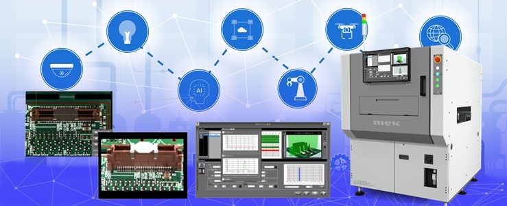
3D AOI Testing For PCB
3D AOI (Automatic Optical Inspection) testing is a type of automated inspection process used in the manufacturing industry to check for defects or irregularities in products or components. It involves the use of specialized equipment, such as 3D cameras or lasers, to scan and analyze the surface of the product or component.
During the inspection process, the 3D AOI equipment compares the scanned image of the product or component to a reference model or design specification. Any deviations from the reference model or specification are identified as defects.
3D AOI testing is often used in the manufacturing of electronics, automotive parts, and medical devices. It can be used to inspect a wide range of products, including printed circuit boards (PCBs), plastic injection molded parts, and metal components.
3D AOI testing is generally faster and more accurate than traditional manual inspection methods, and it can be used to inspect products or components with complex shapes or features that are difficult to inspect manually. It is also less prone to human error, making it a reliable quality control tool in the manufacturing process.

- What is 3D AOI testing?
3D AOI (Automated Optical Inspection) testing is a method of automated inspection that uses advanced imaging technology and algorithms to inspect the surface and internal features of a product or component. It is typically used in the electronics manufacturing industry to ensure that products meet quality standards and specifications.
- How does 3D AOI testing work?
In 3D AOI testing, a high-resolution camera captures images of the product or component from multiple angles. These images are then processed using advanced algorithms to detect defects and deviations from the expected design. The results of the inspection are typically displayed on a computer screen for review by an operator.
- What are the benefits of 3D AOI testing?
There are several benefits to using 3D AOI testing:
- High speed and accuracy: 3D AOI systems can inspect large numbers of products quickly and accurately, reducing the need for manual inspection and increasing the speed of the manufacturing process.
- Increased defect detection: 3D AOI systems can detect defects that may be difficult or impossible for a human inspector to see, such as small cracks or surface defects.
- Reduced inspection costs: Automated inspection reduces the need for manual labor, which can significantly reduce inspection costs.
- Improved product quality: By identifying and correcting defects early in the manufacturing process, 3D AOI testing can help improve the overall quality of the finished product.
- What types of defects can be detected by 3D AOI testing?
3D AOI testing can detect a wide range of defects, including:
- Missing or incorrect components
- Misaligned or improperly positioned components
- Surface defects, such as scratches, dents, or cracks
- Solder defects, such as shorts, opens, or bridging
- Internal defects, such as improper connections or incorrect component placement
- Are there any limitations to 3D AOI testing?
There are a few limitations to 3D AOI testing:
- Cost: 3D AOI systems can be expensive to purchase and maintain.
- Complexity: Some defects may be difficult for the system to detect, especially if they are subtle or hidden.
- False positives: The system may sometimes flag defects that do not actually exist, which can lead to unnecessary rework or wasted time.
- Limited to surface inspection: 3D AOI systems are typically limited to inspecting the surface of a product or component, and may not be able to detect internal defects.
- Dependence on lighting: The accuracy of the inspection may be affected by the lighting conditions in the inspection area.

